In the manufacturing chain of electronic products, the PCBA, as a core component, has its quality and performance directly impacting the final product's market performance. Faced with a wide array of contract manufacturing service providers in the market, making an informed choice has become a focal point for many electronics manufacturers. When selecting a PCBA contract manufacturing service, a comprehensive evaluation from multiple dimensions is necessary to ensure smooth collaboration and reliable product quality.Technical strength is the primary criterion for evaluating a contract manufacturer. A service provider with profound technical expertise can not only offer one-stop services from design to production but also respond swiftly and propose effective solutions when technical challenges arise. This requires the service provider to possess advanced production equipment, precision inspection instruments, and a highly experienced technical team. The level of technical strength is often reflected in its mastery and application of new technologies and processes, as well as its ability to provide customized development based on client needs. Therefore, when selecting, one should thoroughly investigate the service provider's technical background, examine their past project experience—especially cases related to your own product field—to assess technical compatibility.
The PCBA is the core component of electronic devices, and its surface cleanliness directly affects electrical performance and service life. Improper cleaning operations can lead to component damage, loose solder joints, or reduced insulation performance, making it crucial to master the correct cleaning methods. The cleaning process must balance cleaning effectiveness with equipment safety, requiring strict control from tool selection to operational details.The selection of cleaning tools and materials should adhere to the principle of being "gentle and non-damaging." Traditional cotton cloths or ordinary paper towels can easily generate lint, which may remain in circuit board gaps and cause short circuits; it is recommended to use lint-free wipes or specialized anti-static wipes. For cleaning agents, alcohol-based solvents are widely used due to their rapid evaporation and low residue, but attention must be paid to concentration—75% isopropyl alcohol effectively dissolves oils without causing coating peeling on component surfaces due to excessive concentration. For stubborn stains, electronic-grade specialized cleaners can be used, but their compatibility with component materials must be confirmed in advance to prevent corrosive chemicals from contacting sensitive components.
The selection of PCBA thickness is a critical step in the design of electronic products, directly impacting mechanical strength, signal integrity, thermal dissipation efficiency, and cost structure. Different application scenarios have significantly varying requirements for PCBA thickness, necessitating a comprehensive consideration of functional needs, structural constraints, and manufacturing processes to achieve a balance between performance and cost.Mechanical strength is the fundamental consideration in thickness selection. For devices that need to withstand mechanical stress, such as industrial controllers and automotive electronic modules, thicker PCBA boards (2.0mm and above) provide higher resistance to bending and vibration. Such equipment may experience impacts or prolonged vibration during operation; insufficient board thickness can easily lead to solder joint fatigue fracture or loosening of component leads. Conversely, consumer electronic products like smartphones and wearable devices, due to limited internal space and lower mechanical stress, typically use thin boards of 0.8-1.6mm to meet compact structural requirements while reducing overall weight. During design, finite element analysis should be used to simulate mechanical stress distribution and determine the minimum safe thickness, avoiding over-engineering that increases costs.
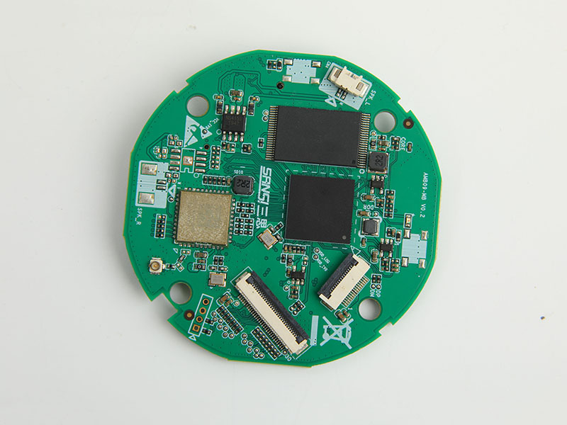
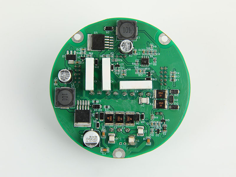
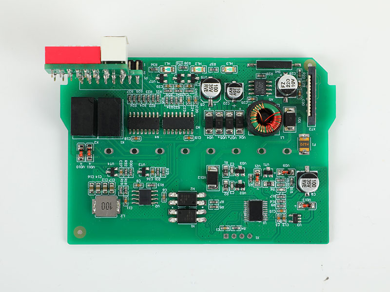
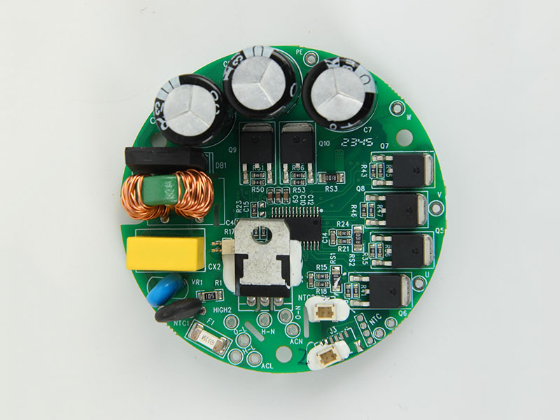
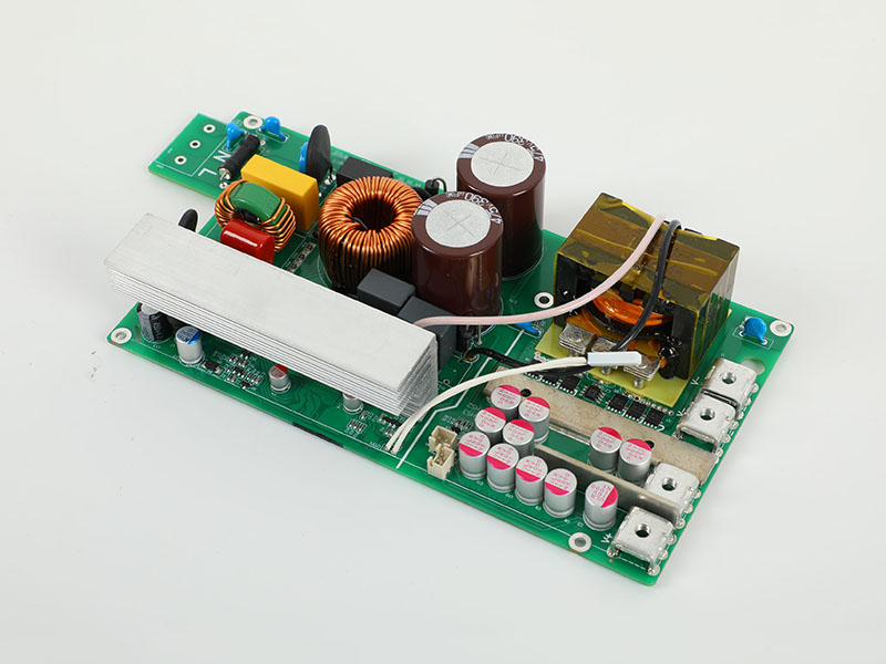
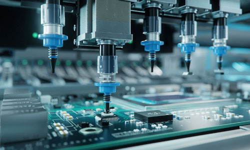
The PCBA production process is the core sequence that integrates electronic components with a Printed Circuit Board (PCB) to form a functional module. Its technical precision and process control directly impact product performance and reliability. From bare board processing to component assembly, and finally to testing and validation, each step must strictly adhere to standardized operations to meet the development demands of miniaturization and high-density integration in electronic products.The starting point of PCBA production is the preparation of the PCB substrate. The PCB substrate is typically made of insulating materials such as epoxy resin fiberglass fabric (FR-4). Its fabrication involves processes including cutting, drilling, electroless copper deposition, pattern transfer, and etching. In the cutting stage, the board is cut to the required dimensions based on design specifications. Drilling uses CNC machines to create component lead holes and vias in the substrate, with hole diameter precision typically controlled within ±0.05mm. The electroless copper deposition process deposits a conductive copper layer on the hole walls, providing a foundation for subsequent electroplating. Pattern transfer uses exposure and development techniques to transfer the designed circuit pattern onto the board surface. Etching then removes unwanted copper foil, forming the precise conductive network. Multi-layer PCBs also require a lamination process to bond inner and outer layers, with laser drilling used to achieve interlayer interconnection.
In the complete chain of PCBA processing, the cost distribution exhibits a distinct gradient characteristic, with the proportion of costs in different stages jointly influenced by product design complexity, production scale, and process requirements. From raw material procurement to final testing, the highest-cost stages are often hidden within seemingly routine processes, where the core contradiction lies at the intersection of technical difficulty, labor dependence, and equipment investment.Electronic component procurement has long occupied the core position of total costs, and its volatility directly impacts project profit margins. The supply stability and price fluctuations of high-end chips are particularly significant; for instance, the unit price of high-performance processors or ASICs may account for more than half of the total component cost. Procurement of such components requires locking in production capacity in advance and is heavily influenced by the international supply chain—prices may double during shortages. In contrast, although passive components like resistors and capacitors have low unit prices, their large quantities mean the total cost remains non-negligible. Controlling component costs requires balancing performance requirements with supply chain risks; excessive pursuit of high-end specifications or excessive cost-cutting may both lead to hidden quality losses.
PCBA Design for Manufacturability (DFM) review is a critical step in the electronic product development process. Its core objective is to reduce defect rates and costs in the manufacturing stage, and improve product yield and production efficiency through proactive design optimization. An effective DFM review must cover four key dimensions: design specifications, process compatibility, assembly feasibility, and testability. Through a systematic inspection process and cross-departmental collaboration, it ensures a seamless transition of the design from blueprint to mass production.Design specification review is the fundamental basis of DFM. It is essential to verify that component placement meets process requirements. For example, the spacing between high-density components must satisfy minimum safety distance standards to prevent bridging during soldering. Large components (such as inductors, transformers) need to be positioned away from the board edge to avoid solder joint cracking caused by mechanical stress during depaneling. For bottom-terminated components like BGAs and QFNs, it is necessary to confirm that the pad design matches the package dimensions, with pad pitch errors controlled within ±0.05mm to ensure uniform solder ball melting during reflow. Additionally, the clarity and reasonable placement of silkscreen markings must be reviewed to avoid assembly errors caused by ambiguous labels.
Total6
Result Pages1 |
This page1 9First page 7Previous Next8 Last Page:
Jump: