4News
Your position: Home ->  News
2026
-
02
-
24
In the manufacturing chain of electronic products, the PCBA, as a core component, has its quality and performance directly impacting the final product's market performance. Faced with a wide array of contract manufacturing service providers in the market, making an informed choice has become a focal point for many electronics manufacturers. When selecting a PCBA contract manufacturing service, a comprehensive evaluation from multiple dimensions is necessary to ensure smooth collaboration and reliable product quality.Technical strength is the primary criterion for evaluating a contract manufacturer. A service provider with profound technical expertise can not only offer one-stop services from design to production but also respond swiftly and propose effective solutions when technical challenges arise. This requires the service provider to possess advanced production equipment, precision inspection instruments, and a highly experienced technical team. The level of technical strength is often reflected in its mastery and application of new technologies and processes, as well as its ability to provide customized development based on client needs. Therefore, when selecting, one should thoroughly investigate the service provider's technical background, examine their past project experience—especially cases related to your own product field—to assess technical compatibility.
2026
-
02
-
24
The PCBA is the core component of electronic devices, and its surface cleanliness directly affects electrical performance and service life. Improper cleaning operations can lead to component damage, loose solder joints, or reduced insulation performance, making it crucial to master the correct cleaning methods. The cleaning process must balance cleaning effectiveness with equipment safety, requiring strict control from tool selection to operational details.The selection of cleaning tools and materials should adhere to the principle of being "gentle and non-damaging." Traditional cotton cloths or ordinary paper towels can easily generate lint, which may remain in circuit board gaps and cause short circuits; it is recommended to use lint-free wipes or specialized anti-static wipes. For cleaning agents, alcohol-based solvents are widely used due to their rapid evaporation and low residue, but attention must be paid to concentration—75% isopropyl alcohol effectively dissolves oils without causing coating peeling on component surfaces due to excessive concentration. For stubborn stains, electronic-grade specialized cleaners can be used, but their compatibility with component materials must be confirmed in advance to prevent corrosive chemicals from contacting sensitive components.
2026
-
02
-
24
The selection of PCBA thickness is a critical step in the design of electronic products, directly impacting mechanical strength, signal integrity, thermal dissipation efficiency, and cost structure. Different application scenarios have significantly varying requirements for PCBA thickness, necessitating a comprehensive consideration of functional needs, structural constraints, and manufacturing processes to achieve a balance between performance and cost.Mechanical strength is the fundamental consideration in thickness selection. For devices that need to withstand mechanical stress, such as industrial controllers and automotive electronic modules, thicker PCBA boards (2.0mm and above) provide higher resistance to bending and vibration. Such equipment may experience impacts or prolonged vibration during operation; insufficient board thickness can easily lead to solder joint fatigue fracture or loosening of component leads. Conversely, consumer electronic products like smartphones and wearable devices, due to limited internal space and lower mechanical stress, typically use thin boards of 0.8-1.6mm to meet compact structural requirements while reducing overall weight. During design, finite element analysis should be used to simulate mechanical stress distribution and determine the minimum safe thickness, avoiding over-engineering that increases costs.
2026
-
02
-
24
The PCBA production process is the core sequence that integrates electronic components with a Printed Circuit Board (PCB) to form a functional module. Its technical precision and process control directly impact product performance and reliability. From bare board processing to component assembly, and finally to testing and validation, each step must strictly adhere to standardized operations to meet the development demands of miniaturization and high-density integration in electronic products.The starting point of PCBA production is the preparation of the PCB substrate. The PCB substrate is typically made of insulating materials such as epoxy resin fiberglass fabric (FR-4). Its fabrication involves processes including cutting, drilling, electroless copper deposition, pattern transfer, and etching. In the cutting stage, the board is cut to the required dimensions based on design specifications. Drilling uses CNC machines to create component lead holes and vias in the substrate, with hole diameter precision typically controlled within ±0.05mm. The electroless copper deposition process deposits a conductive copper layer on the hole walls, providing a foundation for subsequent electroplating. Pattern transfer uses exposure and development techniques to transfer the designed circuit pattern onto the board surface. Etching then removes unwanted copper foil, forming the precise conductive network. Multi-layer PCBs also require a lamination process to bond inner and outer layers, with laser drilling used to achieve interlayer interconnection.
2026
-
02
-
24
In the complete chain of PCBA processing, the cost distribution exhibits a distinct gradient characteristic, with the proportion of costs in different stages jointly influenced by product design complexity, production scale, and process requirements. From raw material procurement to final testing, the highest-cost stages are often hidden within seemingly routine processes, where the core contradiction lies at the intersection of technical difficulty, labor dependence, and equipment investment.Electronic component procurement has long occupied the core position of total costs, and its volatility directly impacts project profit margins. The supply stability and price fluctuations of high-end chips are particularly significant; for instance, the unit price of high-performance processors or ASICs may account for more than half of the total component cost. Procurement of such components requires locking in production capacity in advance and is heavily influenced by the international supply chain—prices may double during shortages. In contrast, although passive components like resistors and capacitors have low unit prices, their large quantities mean the total cost remains non-negligible. Controlling component costs requires balancing performance requirements with supply chain risks; excessive pursuit of high-end specifications or excessive cost-cutting may both lead to hidden quality losses.
2026
-
02
-
24
PCBA Design for Manufacturability (DFM) review is a critical step in the electronic product development process. Its core objective is to reduce defect rates and costs in the manufacturing stage, and improve product yield and production efficiency through proactive design optimization. An effective DFM review must cover four key dimensions: design specifications, process compatibility, assembly feasibility, and testability. Through a systematic inspection process and cross-departmental collaboration, it ensures a seamless transition of the design from blueprint to mass production.Design specification review is the fundamental basis of DFM. It is essential to verify that component placement meets process requirements. For example, the spacing between high-density components must satisfy minimum safety distance standards to prevent bridging during soldering. Large components (such as inductors, transformers) need to be positioned away from the board edge to avoid solder joint cracking caused by mechanical stress during depaneling. For bottom-terminated components like BGAs and QFNs, it is necessary to confirm that the pad design matches the package dimensions, with pad pitch errors controlled within ±0.05mm to ensure uniform solder ball melting during reflow. Additionally, the clarity and reasonable placement of silkscreen markings must be reviewed to avoid assembly errors caused by ambiguous labels.
2026
-
02
-
24
In the field of medical devices, the PCBA, as a core component, has its performance and reliability directly impacting patient safety and treatment outcomes. Compared to consumer electronics or industrial equipment, PCBA for medical applications must meet more stringent standards, covering multiple dimensions including material selection, process control, environmental adaptability, and safety certifications.Medical PCBA has extremely high requirements for material stability. Medical devices often need to operate in environments with high temperatures, high humidity, or frequent disinfection. Ordinary PCB substrates are prone to deformation or performance degradation due to thermal expansion and contraction. Therefore, the medical field commonly uses materials with a high glass transition temperature (Tg). Such materials maintain structural stability even at high temperatures, preventing circuit failures caused by environmental changes. Simultaneously, to prevent degradation of insulation performance in humid environments, the materials must possess low moisture absorption properties, ensuring signal transmission stability. Furthermore, medical devices have strict requirements for the biocompatibility of materials, especially for implantable devices or components that come into direct contact with the human body. Their substrates, solders, and encapsulation materials must pass biological tests such as cytotoxicity and skin irritation to avoid allergic or toxic reactions.
2026
-
02
-
24
In today's world of increasing electronic product prevalence, the PCBA board (Printed Circuit Board Assembly) serves as a core component, and its operational lifespan directly impacts the overall reliability and durability of the product. Effectively extending the service life of a PCBA board not only enhances user experience but also reduces resource waste, aligning with the principles of sustainable development. The following discussion will explore multiple strategies to effectively prolong the lifespan of PCBA boards within products.Reasonable design is the foundation for extending the operational life of a PCBA board. During the design phase, full consideration should be given to the board's operating environment and load conditions to select appropriate components and materials. For instance, PCBA boards intended for high-temperature or high-humidity environments should utilize components and packaging with enhanced heat resistance and moisture protection, thereby mitigating damage from environmental factors. Concurrently, optimizing circuit layout and routing to minimize signal interference and electromagnetic radiation reduces the risk of component failure due to unstable operation.
2026
-
02
-
24
PCBA board, which stands for Printed Circuit Board Assembly, is an indispensable core component in modern electronic devices, serving the functions of component mounting and electrical interconnection. Designing a high-quality PCBA requires not only a solid foundation in electronics but also an in-depth understanding of the design process, component selection, layout and routing, and various other aspects. The following introduces some fundamental knowledge of PCBA design.PCBA design begins with clearly defined design requirements and specifications. This includes determining the product's functional positioning, performance targets, operating environment, and cost budget. Clear requirement analysis is the first step toward successful design, directly influencing subsequent component selection, circuit design, and PCB layout. Designers must communicate closely with clients or the product team to ensure a comprehensive and accurate understanding of the requirements.
2026
-
02
-
24
During the production of PCBA boards, copper surface oxidation is a critical issue affecting circuit reliability. Copper, as the core material for conductive layers, suffers from reduced conductivity due to surface oxidation, leading to poor soldering and even signal degradation during long-term use. From raw material storage to processing stages and post-treatment processes, systematic control measures are required to interrupt the oxidation chain and ensure the copper surface remains clean over time.Protection during raw material storage serves as the first line of defense against oxidation. Copper foil rolls, before processing, must be stored in a dry, sealed environment. Controlling humidity below 30% effectively inhibits oxidation reactions. Storage containers should be made of moisture-proof materials with anti-oxidation coatings applied to inner walls to prevent direct contact between copper and air. For opened copper foil, packaging bags should be filled with nitrogen and sealed, using inert gas to isolate oxygen and moisture. A factory comparison once revealed that copper foil stored in humid environments for one week without special treatment developed a surface oxide layer three times thicker, while nitrogen-packaged equivalent material showed almost no change in oxidation layer thickness.
2026
-
02
-
24
As a core component of electronic products, the PCBA board directly impacts product performance and reliability. To ensure stable operation of PCBA boards in complex environments, multi-dimensional inspection methods are required to comprehensively evaluate their performance. The following systematically outlines key PCBA board inspection methods, ranging from basic visual inspection to in-depth reliability testing.Basic visual inspection serves as the first checkpoint for quality control. Traditional visual inspection relies on operator experience, using magnifying glasses or microscopes to observe details such as component polarity, solder joint morphology, and PCB surface scratches. Although this method is low-cost, the identification of minor defects is susceptible to subjective factors. The introduction of Automated Optical Inspection (AOI) addresses this challenge by utilizing high-resolution cameras to capture PCBA images and algorithmically comparing them against standard templates, enabling rapid identification of defects such as component misalignment, poor solder joints, and bridging. Inspection efficiency is several times higher than manual methods, making it particularly suitable for high-volume production scenarios.
2026
-
02
-
24
As a core component of electronic products, the PCBA board's quality and performance stability directly impact the overall reliability and service life of the end product. During the production, transportation, and storage of PCBA boards, the storage environment is a critical factor that is easily overlooked. Improper storage conditions can lead to moisture absorption, oxidation, short circuits, and even functional failure of the PCBA board. Therefore, understanding and adhering to the storage environment requirements for PCBA boards is particularly necessary.PCBA boards have strict requirements regarding storage temperature. Temperatures that are too high or too low can cause damage. High temperatures accelerate the aging process of components, especially plastic-encapsulated ones, which may crack or deform due to differences in the coefficient of thermal expansion. Simultaneously, high temperatures can potentially reflow solder, causing loose connections or short circuits. Conversely, low temperatures can make certain components brittle and susceptible to damage, and moisture in the air is more likely to condense as frost, increasing the risk of moisture absorption. Therefore, PCBA boards should be stored in an environment with suitable temperature and minimal fluctuation; a general recommendation is a temperature range between 5°C and 30°C.
2026
-
02
-
24
In the development process of electronic products, the design phase of the PCBA is of paramount importance. It not only dictates the product's performance but also directly impacts the feasibility and cost-effectiveness of subsequent production. When designing a PCBA, numerous details must be meticulously considered to ensure the final product is stable, reliable, and suitable for efficient manufacturing.The rationality of the circuit layout is the cornerstone of PCBA design. A well-planned layout can effectively reduce signal interference and enhance circuit stability. During design, the signal flow principle should be followed, with high-frequency signals logically separated from low-frequency signals, and digital signals from analog signals, placing them in distinct zones to avoid mutual interference. Simultaneously, critical components such as processors and power modules should be positioned in locations with good heat dissipation and easy access for maintenance, ensuring stable performance over the long term. Furthermore, the spacing between components must be considered during layout to prevent soldering shorts caused by excessive proximity or signal attenuation due to excessive distance.
2026
-
02
-
24
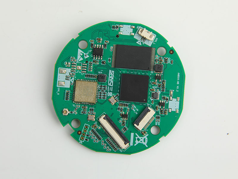
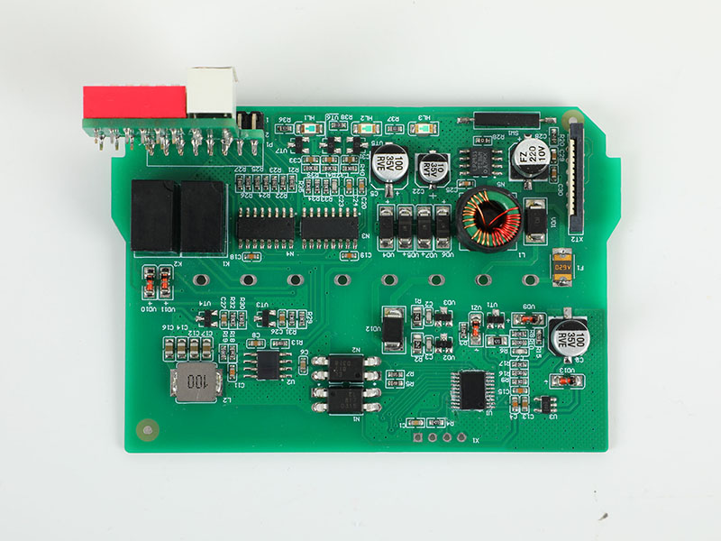
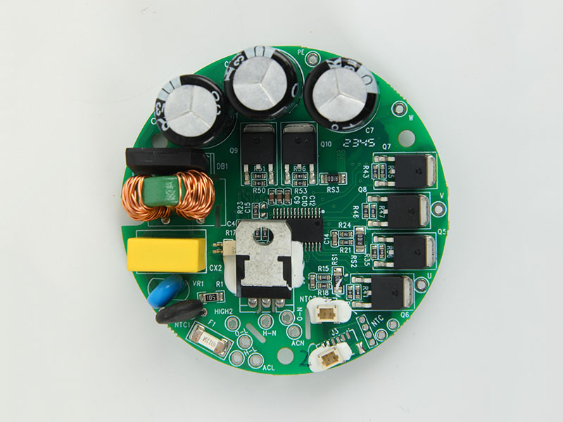
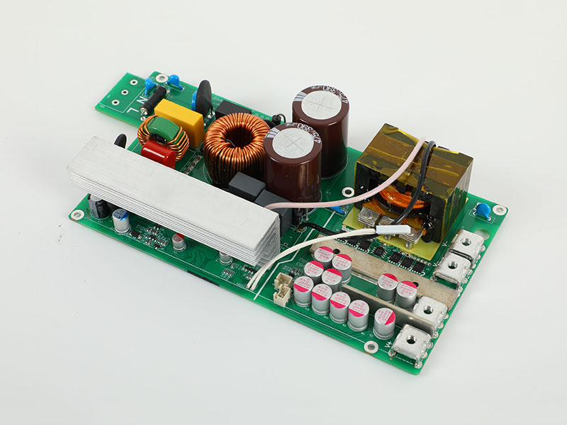
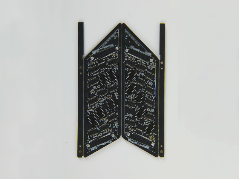
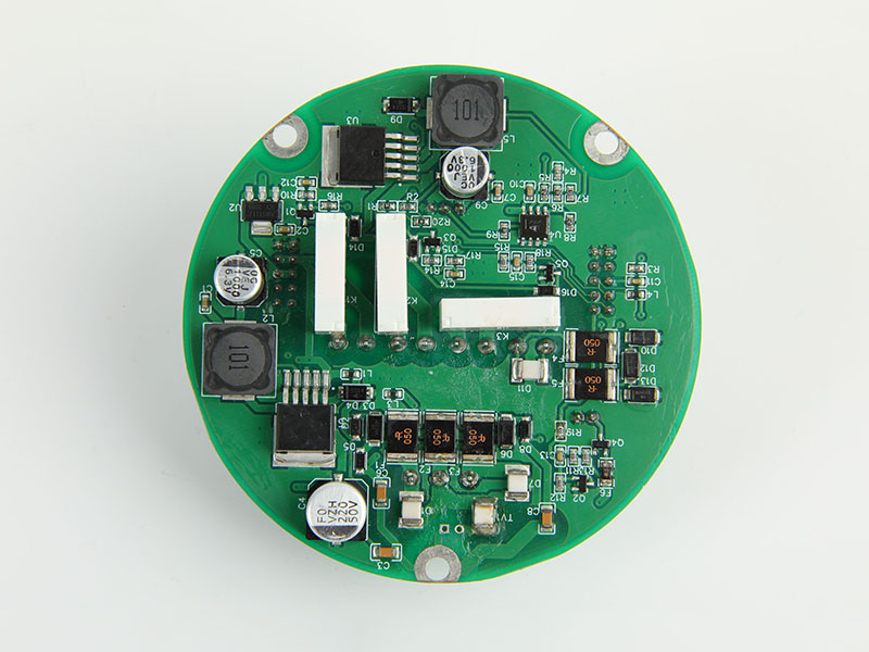
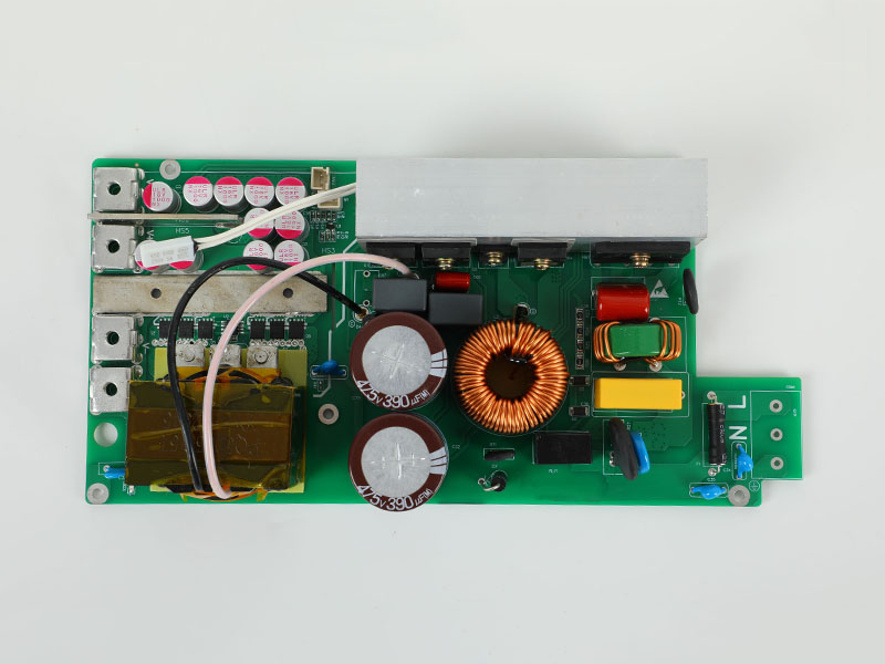
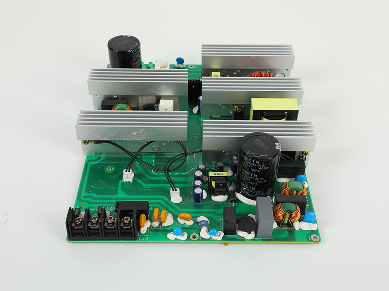
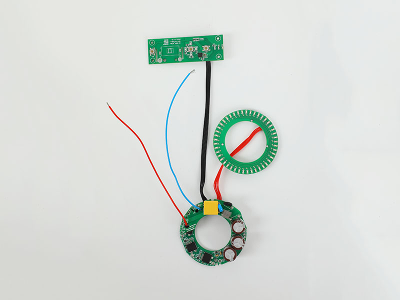
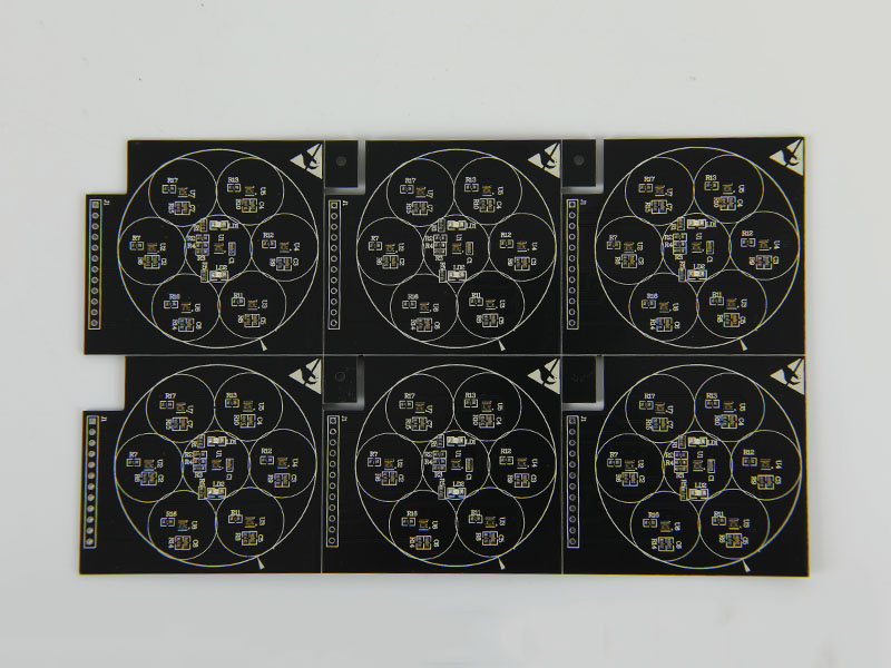
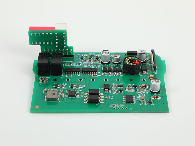
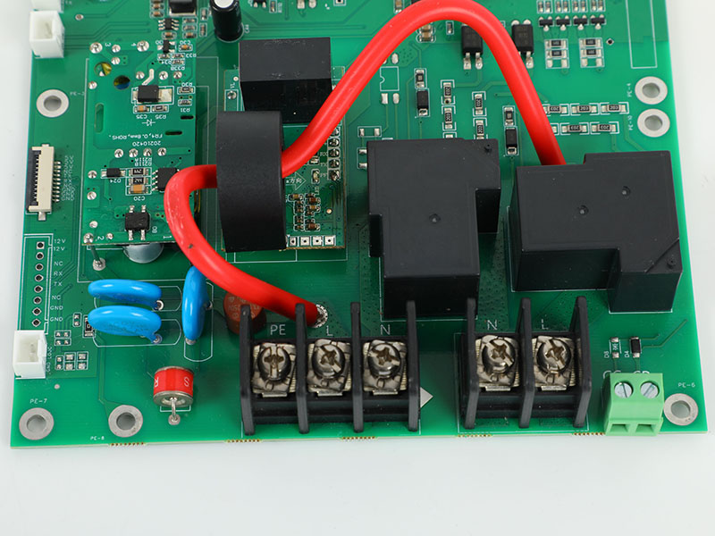
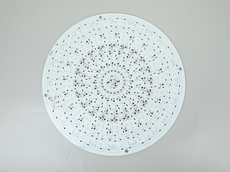
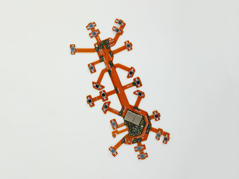
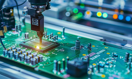
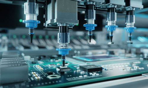
PCBA, or Printed Circuit Board Assembly, is the physical foundation that carries the core functions in modern electronic devices. It integrates electronic components with a Printed Circuit Board (PCB) through soldering processes to form a complete module with specific electrical performance. From smartphones to industrial controllers, from home appliances to aerospace equipment, PCBA supports the operation of various electronic products in a highly integrated and standardized form. Its design, manufacturing, and quality directly determine the performance and reliability of the final product.The composition of a PCBA can be divided into two core parts: the PCB substrate and the electronic components. The PCB substrate is typically made from insulating materials such as epoxy resin fiberglass fabric (FR-4), with a layer of copper foil covering its surface to form the conductive circuitry. Through the etching process, the copper foil is transformed into a complex network of traces, enabling signal transmission and power distribution. Based on the number of layers, PCBs can be classified as single-layer, double-layer, or multi-layer boards. Multi-layer boards, utilizing inner layer traces and via designs, achieve higher component density and more complex circuit functions. Electronic components, including chips, resistors, capacitors, inductors, connectors, etc., are then fixed onto the PCB using Surface Mount Technology (SMT) or Through-Hole Technology (THT), collectively forming a complete circuit system.
2026
-
02
-
24
As the core component of electronic devices, the performance stability of the PCBA is directly related to the overall operational effectiveness of the equipment. Daily maintenance not only extends the service life of the PCBA but also reduces equipment failure rates and lowers maintenance costs. From environmental control to operational specifications, from cleaning maintenance to storage management, scientific care should be integrated throughout the entire lifecycle of the PCBA.Environmental control is the foundation of PCBA maintenance. Temperature, humidity, and dust are the three main environmental factors affecting its performance. High temperatures can accelerate component aging, while low temperatures may cause solder joints to become brittle; therefore, PCBA should be stored in a constant temperature environment of 15-35°C. Excessive humidity can easily lead to oxidation and corrosion of metal parts, while too low humidity may generate static electricity; it is recommended to control relative humidity within the 40%-60% range. Dust accumulation can reduce heat dissipation efficiency and may even cause short circuits, so PCBA must be kept away from dust sources, and protective covers or sealed cabinets should be used when necessary. A laboratory comparison found that PCBA without dust protection experienced a 30% decrease in heat dissipation efficiency after six months of operation, while similar products with regular cleaning maintained stable performance.
2026
-
02
-
24
As the core component of electronic products, the quality stability of the PCBA directly affects the functionality and lifespan of the equipment. However, during actual production or use, PCBA may sometimes experience cracking or voiding phenomena. These issues not only impact circuit performance but can also pose safety hazards. An in-depth analysis of their causes helps to avoid risks at the source and improve product reliability.Common causes of PCBA cracking are often related to material selection and process control. The substrate material is a key factor affecting resistance to cracking. If a material with a low Tg (glass transition temperature) is chosen, the substrate may soften and lose structural strength in high-temperature environments, leading to cracking at points of stress concentration. For example, during reflow or wave soldering, if the temperature profile is set improperly, localized overheating can cause a significant difference in the expansion coefficient between the substrate and components, generating internal stress that may lead to cracking after long-term use. Additionally, mechanical stress is an important contributing factor. If the PCBA is subjected to severe vibration, impact, or bending during assembly, transportation, or use that exceeds the material's tolerance limit, the substrate or solder joints may crack. For instance, failing to reserve sufficient mechanical buffer space during design, or placing components too densely, can reduce the overall impact resistance.
2026
-
02
-
24
As the core component of electronic products, the installation quality of the PCBA directly affects the overall performance and stability of the finished product. To ensure the installation process is standardized and orderly, and to enhance product quality, following a scientific and reasonable installation procedure is particularly important. The following details the standard procedure for PCBA installation, aiming to provide a reference for relevant practitioners.Before installing the PCBA, preparation work is an indispensable step. This includes a thorough inspection of the installation environment to ensure the work area is clean, tidy, dust-free, and static-free, preventing dust or static electricity from damaging sensitive electronic components. Simultaneously, all necessary installation tools, such as anti-static wrist straps, precision screwdrivers, and soldering equipment, must be prepared and confirmed to be in good condition for precise operation. Additionally, a visual inspection of the PCBA itself is necessary to confirm there is no damage or missing components, laying a solid foundation for subsequent installation.
2026
-
02
-
24
PCBA, or Printed Circuit Board Assembly, is an indispensable core component in modern electronic products. Its processing workflow is complex and delicate, with each step directly impacting the quality and performance of the final product. The following details the main process flow of PCBA processing and the key precautions to be observed during this procedure.PCBA processing begins with the preparation of the PCB board. In this step, the substrate must be precisely cut to the required dimensions according to the design drawings. Subsequently, complex circuit patterns are formed on the substrate through techniques such as chemical etching or laser engraving. Precision is of utmost importance in this process, as any minor deviation can affect the subsequent installation of components and the connectivity of the circuits. Therefore, operators must possess a high level of professional skill, and simultaneously, the equipment must be maintained in a high-precision state with regular calibration and upkeep to ensure processing quality.
   Total18  Result Pages1 | This page1  9First page   7Previous   Next8   Last Page:  Jump: