The PCBA production process is the core sequence that integrates electronic components with a Printed Circuit Board (PCB) to form a functional module. Its technical precision and process control directly impact product performance and reliability. From bare board processing to component assembly, and finally to testing and validation, each step must strictly adhere to standardized operations to meet the development demands of miniaturization and high-density integration in electronic products.
The starting point of PCBA production is the preparation of the PCB substrate. The PCB substrate is typically made of insulating materials such as epoxy resin fiberglass fabric (FR-4). Its fabrication involves processes including cutting, drilling, electroless copper deposition, pattern transfer, and etching. In the cutting stage, the board is cut to the required dimensions based on design specifications. Drilling uses CNC machines to create component lead holes and vias in the substrate, with hole diameter precision typically controlled within ±0.05mm. The electroless copper deposition process deposits a conductive copper layer on the hole walls, providing a foundation for subsequent electroplating. Pattern transfer uses exposure and development techniques to transfer the designed circuit pattern onto the board surface. Etching then removes unwanted copper foil, forming the precise conductive network. Multi-layer PCBs also require a lamination process to bond inner and outer layers, with laser drilling used to achieve interlayer interconnection.
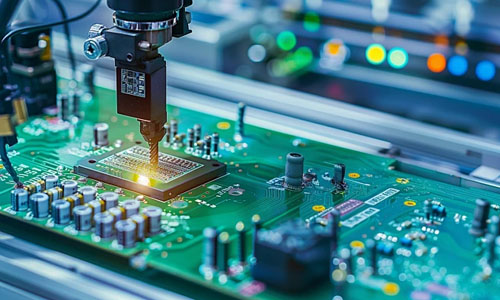
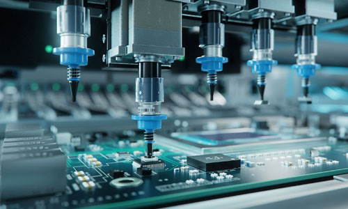
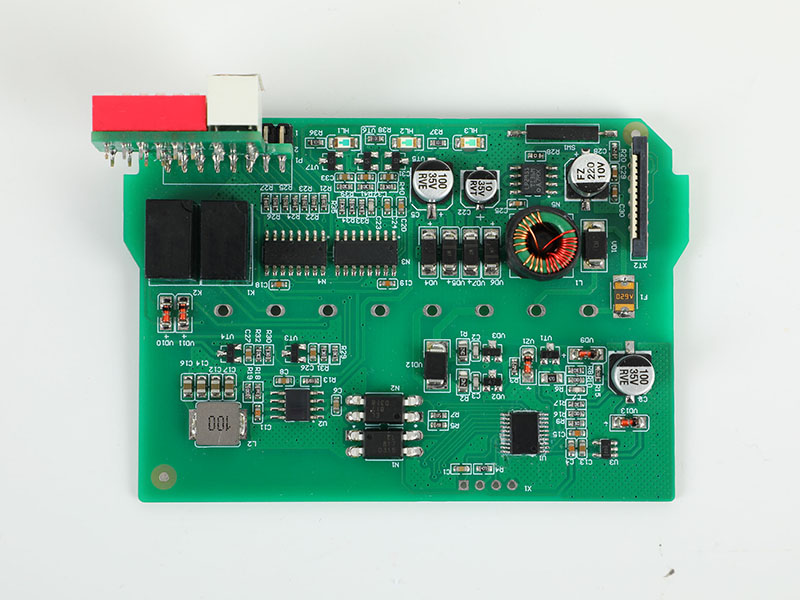
Component assembly is the core step of PCBA production, primarily divided into Surface Mount Technology (SMT) and Through-Hole Technology (THT). The SMT process is suitable for miniature components (such as 0201-sized resistors, BGA chips), and its workflow includes solder paste printing, component placement, and reflow soldering. Solder paste printing uses a stencil to accurately deposit solder paste onto the pads; the stencil thickness and aperture size directly influence the solder paste volume—too thick can easily cause shorts, while too thin may lead to insufficient solder joints. Pick-and-place machines use vision alignment systems to pick up components and place them precisely on the designated pads, achieving accuracy within ±0.03mm. Reflow soldering involves controlling a temperature profile to melt and solidify the solder paste, forming reliable electrical connections. The THT process is for leaded components (such as electrolytic capacitors, connectors), requiring components to be inserted into plated through-holes before being secured via wave soldering or manual soldering. Wave soldering uses a molten solder wave to solder the leads, while manual soldering relies on operator experience and is suitable for complex layouts or scenarios demanding high reliability.
Post-soldering cleaning and inspection stages are equally critical. Flux residues can potentially corrode circuits or cause conductive failures, hence they must be removed using cleaning equipment. Cleaning methods include water cleaning and no-clean processes; the former requires deionized water and cleaning agents, while the latter relies on low-residue fluxes. The inspection phase encompasses visual inspection, electrical testing, and functional validation. Visual inspection, performed manually or via Automated Optical Inspection (AOI) equipment, identifies solder joint defects (such as bridging, insufficient solder). Electrical testing, using flying probe testers or In-Circuit Testers (ICT), verifies circuit continuity. Functional testing simulates actual operating conditions to ensure the PCBA meets design specifications.
As electronic products evolve towards higher density and performance, PCBA production processes continuously advance. High-Density Interconnect (HDI) technology utilizes laser blind vias and microvias to achieve finer trace geometries and smaller component pitches. The application of Flexible PCBs (FPC) and Rigid-Flex boards allows PCBA to adapt to bending or folding scenarios. Embedded component technology integrates chips directly into the PCB substrate, further saving space and enhancing signal transmission efficiency. These technological breakthroughs not only increase the integration level of PCBA but also provide essential hardware support for the development of emerging fields like 5G communication, artificial intelligence, and the Internet of Things.
The PCBA production process forms the foundation of electronics manufacturing; its technical depth and process precision directly determine a product's market competitiveness. From substrate preparation to component assembly, and through to cleaning and inspection, each stage requires balancing efficiency, cost, and quality to meet ever-increasing technical challenges.


No. 501, Industrial North Area, Xinhé Community, Fuhai Subdistrict, Bao'an District, Shenzhen City, Guangdong Province, China