PCBA board, which stands for Printed Circuit Board Assembly, is an indispensable core component in modern electronic devices, serving the functions of component mounting and electrical interconnection. Designing a high-quality PCBA requires not only a solid foundation in electronics but also an in-depth understanding of the design process, component selection, layout and routing, and various other aspects. The following introduces some fundamental knowledge of PCBA design.
PCBA design begins with clearly defined design requirements and specifications. This includes determining the product's functional positioning, performance targets, operating environment, and cost budget. Clear requirement analysis is the first step toward successful design, directly influencing subsequent component selection, circuit design, and PCB layout. Designers must communicate closely with clients or the product team to ensure a comprehensive and accurate understanding of the requirements.
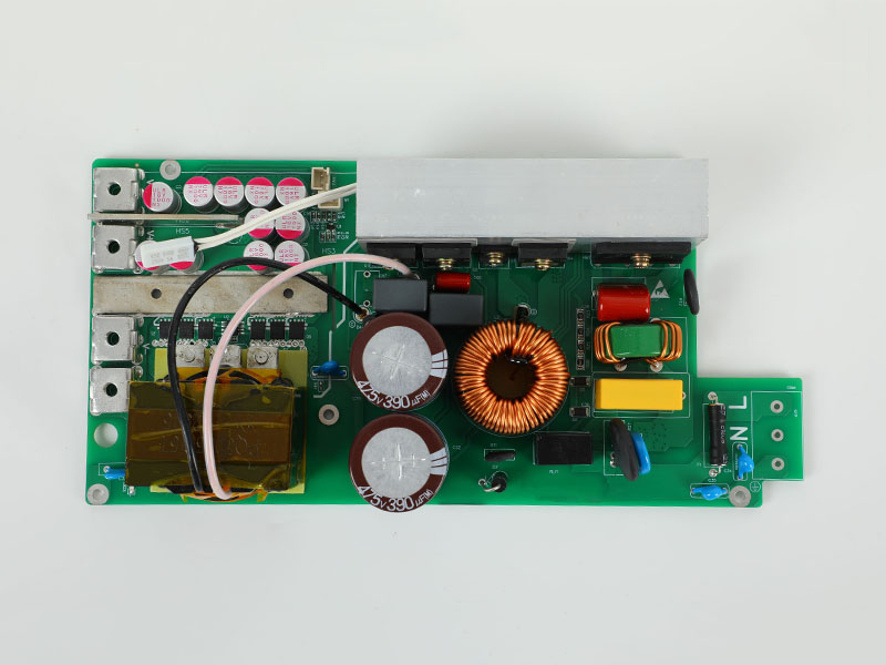
Component selection is a critical phase in PCBA design. The right components not only meet the product's functional needs but also achieve an optimal balance in terms of cost, reliability, and supply chain continuity. Designers need to screen components based on circuit requirements, selecting those with matching performance parameters and appropriate packaging. Furthermore, attention must be paid to component supply stability and life cycle to avoid production interruptions or premature product obsolescence due to shortages or discontinuation. During the selection process, factors such as power consumption, thermal dissipation needs, and compatibility with other components should also be considered.
Layout and routing form the core of PCBA design, directly impacting circuit performance and stability. During layout, the principle of signal flow should be followed, with high-frequency signals, low-frequency signals, digital signals, and analog signals placed in distinct areas to minimize interference. Critical components such as processors and power modules should be positioned where heat dissipation is effective and maintenance is convenient. When routing, parameters like trace width, spacing, and via size must be carefully considered to ensure signal transmission stability and impedance matching. For high-speed signal lines, special techniques such as differential routing and impedance control are necessary to reduce signal attenuation and crosstalk.
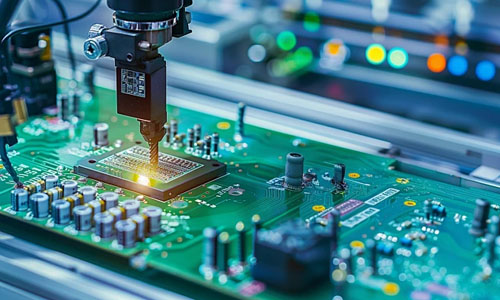
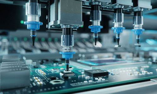
PCBA design must also account for manufacturability and testability. The design should aim to simplify production processes, reduce unnecessary manufacturing steps, and lower production costs. For example, selecting appropriate component packaging types and avoiding overly complex or specialized packages can reduce soldering difficulty and cost. Additionally, sufficient test points should be reserved during design to facilitate subsequent functional testing and troubleshooting. Test points should be logically arranged, easily accessible, and should not interfere with the normal operation of the circuit.
PCBA design is a comprehensive process that requires designers to possess a solid foundation in electronics, keen market insight, and extensive practical experience. Through continuous learning and practice, designers can gradually master the essence of PCBA design, creating high-quality PCBA boards with stable performance, reasonable cost, and ease of production and maintenance, thereby contributing to the advancement of modern electronic devices.


No. 501, Industrial North Area, Xinhé Community, Fuhai Subdistrict, Bao'an District, Shenzhen City, Guangdong Province, China