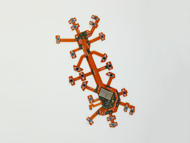
PCBA, or Printed Circuit Board Assembly, is an indispensable core component in modern electronic products. Its processing workflow is complex and delicate, with each step directly impacting the quality and performance of the final product. The following details the main process flow of PCBA processing and the key precautions to be observed during this procedure.
PCBA processing begins with the preparation of the PCB board. In this step, the substrate must be precisely cut to the required dimensions according to the design drawings. Subsequently, complex circuit patterns are formed on the substrate through techniques such as chemical etching or laser engraving. Precision is of utmost importance in this process, as any minor deviation can affect the subsequent installation of components and the connectivity of the circuits. Therefore, operators must possess a high level of professional skill, and simultaneously, the equipment must be maintained in a high-precision state with regular calibration and upkeep to ensure processing quality.
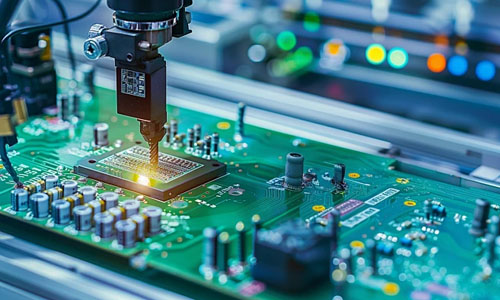
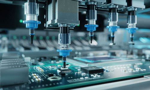
After the PCB preparation is completed, the next step is the component placement stage. This step is typically carried out using automated pick-and-place machines, which can quickly and accurately place various electronic components onto the designated positions on the PCB board. During this process, special attention must be paid to the polarity and orientation of components to avoid circuit shorts or functional failures caused by incorrect placement. Furthermore, for components of different sizes and shapes, appropriate suction nozzles and placement parameters must be selected to ensure secure attachment without causing damage to the components.
Once placement is finished, the process moves to the soldering stage. Soldering is a critical step in PCBA processing, directly related to the stability of the electrical connection between the components and the PCB board. Modern PCBA processing commonly employs reflow soldering or wave soldering techniques. Reflow soldering is suitable for surface mount components, using heat to melt the solder paste and form reliable solder joints; wave soldering is suitable for through-hole components, achieving soldering through the wetting action of a molten solder wave. Regardless of the technique used, the soldering temperature and time must be strictly controlled to avoid component damage or weak joints due to overheating, while also preventing poor contact caused by insufficient soldering.
After soldering is complete, the PCBA must undergo cleaning and inspection. Cleaning aims to remove flux residues and impurities generated during the soldering process, preventing them from affecting circuit performance. The inspection phase uses methods such as visual inspection, Automated Optical Inspection (AOI), or X-ray inspection to confirm whether solder joint quality, component placement positions, and circuit connectivity meet the requirements. Any problems discovered must be promptly documented, their causes analyzed, and appropriate measures taken for repair or adjustment.
Throughout the entire PCBA processing workflow, special attention must also be paid to environmental control. The processing workshop should maintain constant temperature and humidity to minimize the impact of dust and static electricity on the process. Simultaneously, operators must wear anti-static clothing and gloves to prevent human-body electrostatic discharge from damaging sensitive electronic components. By implementing these meticulous precautions, the efficiency and stability of the PCBA processing can be ensured, ultimately producing high-quality, high-performance electronic products.


No. 501, Industrial North Area, Xinhé Community, Fuhai Subdistrict, Bao'an District, Shenzhen City, Guangdong Province, China