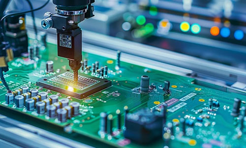
In the development process of electronic products, the design phase of the PCBA is of paramount importance. It not only dictates the product's performance but also directly impacts the feasibility and cost-effectiveness of subsequent production. When designing a PCBA, numerous details must be meticulously considered to ensure the final product is stable, reliable, and suitable for efficient manufacturing.
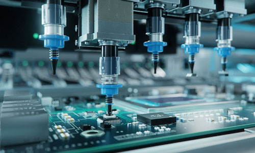
The rationality of the circuit layout is the cornerstone of PCBA design. A well-planned layout can effectively reduce signal interference and enhance circuit stability. During design, the signal flow principle should be followed, with high-frequency signals logically separated from low-frequency signals, and digital signals from analog signals, placing them in distinct zones to avoid mutual interference. Simultaneously, critical components such as processors and power modules should be positioned in locations with good heat dissipation and easy access for maintenance, ensuring stable performance over the long term. Furthermore, the spacing between components must be considered during layout to prevent soldering shorts caused by excessive proximity or signal attenuation due to excessive distance.
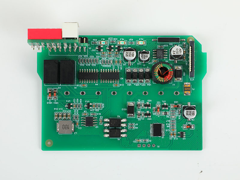
Component selection requires balancing performance and cost. Choosing cost-effective components while meeting the product's functional requirements is key to lowering costs and enhancing competitiveness. Designers need a deep understanding of component performance parameters, such as operating voltage, current, and frequency response, to ensure the selected components function reliably within the design environment. Attention must also be paid to the component's package type and dimensions to ensure compatibility with the PCB layout, facilitating subsequent soldering and assembly. Additionally, the supply stability and lifecycle of components are factors that cannot be overlooked, preventing production interruptions due to component shortages or discontinuation.
Power and grounding design is another critical aspect for ensuring stable circuit operation. A well-executed power design provides a stable and clean power supply, minimizing the impact of power supply noise on the circuit. During design, power paths should be carefully planned, and appropriate filtering measures, such as using capacitors and inductors to filter out high-frequency noise from the power supply, should be implemented. Grounding design is equally crucial; a proper grounding method can effectively reduce ground impedance and minimize interference caused by ground loops. Designers must select an appropriate grounding strategy based on circuit characteristics, such as single-point grounding, multi-point grounding, or hybrid grounding.
Design for Manufacturability (DFM) and Design for Testability (DFT) are also critical factors to consider during the design phase. When designing a PCBA, full consideration must be given to the process requirements of production, such as component soldering methods, PCB layer count and thickness, and hole sizes, ensuring the design is easy to manufacture and reduces production costs. Simultaneously, sufficient test points must be reserved during design to facilitate subsequent functional testing and fault diagnosis. The layout of test points should be reasonable, easily accessible, and should not interfere with the normal operation of the circuit.
Designing a PCBA is a meticulous process that requires comprehensive consideration of multiple aspects, including circuit layout, component selection, power and grounding design, as well as Design for Manufacturability and Design for Testability.


No. 501, Industrial North Area, Xinhé Community, Fuhai Subdistrict, Bao'an District, Shenzhen City, Guangdong Province, China