PCBA, or Printed Circuit Board Assembly, is the physical foundation that carries the core functions in modern electronic devices. It integrates electronic components with a Printed Circuit Board (PCB) through soldering processes to form a complete module with specific electrical performance. From smartphones to industrial controllers, from home appliances to aerospace equipment, PCBA supports the operation of various electronic products in a highly integrated and standardized form. Its design, manufacturing, and quality directly determine the performance and reliability of the final product.
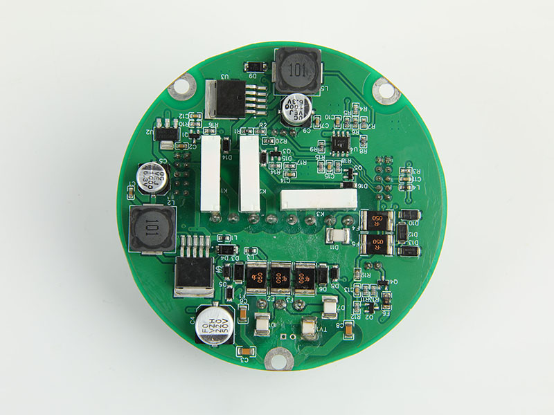
The composition of a PCBA can be divided into two core parts: the PCB substrate and the electronic components. The PCB substrate is typically made from insulating materials such as epoxy resin fiberglass fabric (FR-4), with a layer of copper foil covering its surface to form the conductive circuitry. Through the etching process, the copper foil is transformed into a complex network of traces, enabling signal transmission and power distribution. Based on the number of layers, PCBs can be classified as single-layer, double-layer, or multi-layer boards. Multi-layer boards, utilizing inner layer traces and via designs, achieve higher component density and more complex circuit functions. Electronic components, including chips, resistors, capacitors, inductors, connectors, etc., are then fixed onto the PCB using Surface Mount Technology (SMT) or Through-Hole Technology (THT), collectively forming a complete circuit system.
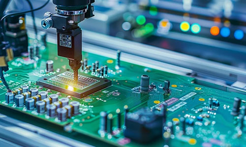
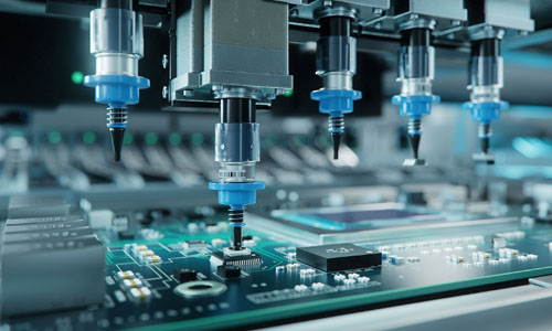
The PCBA manufacturing process encompasses several precision stages. First, the PCB substrate must be fabricated according to the circuit design, involving processes such as cutting, drilling, electroless copper deposition, pattern transfer, and etching to ensure trace accuracy and via reliability. This is followed by the component assembly stage, where the SMT process uses high-speed pick-and-place machines to accurately place miniature components onto the pads, while the THT process involves inserting leaded components into plated through-holes and securing them through manual soldering or wave soldering. After soldering, cleaning is required to remove flux residues, preventing corrosion or short circuits. Finally, functional testing and reliability validation are conducted to ensure the PCBA meets design specifications, including electrical performance tests and environmental adaptability tests such as thermal cycling and vibration testing.
The design of a PCBA must balance electrical performance with manufacturing feasibility. Electrical design requires optimizing trace layout to minimize signal interference and transmission loss; for example, high-frequency signals require differential routing and impedance control, while power supply traces may need increased copper thickness to reduce resistance. Manufacturing feasibility involves considerations of component placement and process compatibility, such as reserving sufficient soldering space for high-density components and designing dedicated fixtures to assist in the assembly of oddly-shaped components. Furthermore, thermal design is a critical aspect; power components need thermal pads or thermal vias to dissipate heat, preventing localized overheating that could lead to performance degradation or component damage.
As electronic products evolve towards miniaturization and higher performance, the technological trends in PCBA are increasingly evident. High-Density Interconnect (HDI) technology, through laser drilling and micro-via designs, achieves finer trace geometries and smaller component pitches. The application of Flexible PCBs (FPC) and Rigid-Flex boards allows PCBA to adapt to bending or folding scenarios, such as in wearable devices and foldable smartphones. Embedded component technology integrates chips directly into the PCB substrate, further saving space and enhancing signal transmission efficiency. These technological breakthroughs continuously expand the application boundaries of PCBA, driving the electronics industry towards higher integration and lower power consumption.
As the "neural center" of electronic products, the technical depth and manufacturing precision of PCBA directly determine a product's market competitiveness. From design optimization to process innovation, from quality control to cost balancing, the evolution of PCBA mirrors the technological progress of the electronics industry and lays the physical foundation for future development towards intelligence and the Internet of Things.


No. 501, Industrial North Area, Xinhé Community, Fuhai Subdistrict, Bao'an District, Shenzhen City, Guangdong Province, China