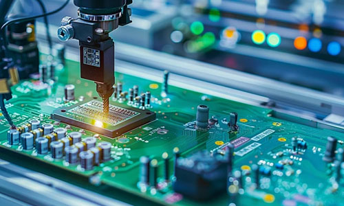
As the core component of electronic products, the quality stability of the PCBA directly affects the functionality and lifespan of the equipment. However, during actual production or use, PCBA may sometimes experience cracking or voiding phenomena. These issues not only impact circuit performance but can also pose safety hazards. An in-depth analysis of their causes helps to avoid risks at the source and improve product reliability.
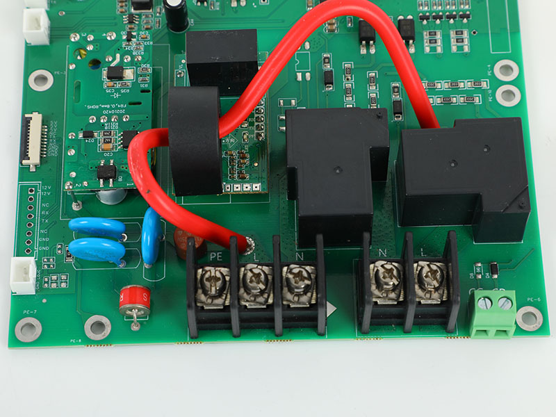
Common causes of PCBA cracking are often related to material selection and process control. The substrate material is a key factor affecting resistance to cracking. If a material with a low Tg (glass transition temperature) is chosen, the substrate may soften and lose structural strength in high-temperature environments, leading to cracking at points of stress concentration. For example, during reflow or wave soldering, if the temperature profile is set improperly, localized overheating can cause a significant difference in the expansion coefficient between the substrate and components, generating internal stress that may lead to cracking after long-term use. Additionally, mechanical stress is an important contributing factor. If the PCBA is subjected to severe vibration, impact, or bending during assembly, transportation, or use that exceeds the material's tolerance limit, the substrate or solder joints may crack. For instance, failing to reserve sufficient mechanical buffer space during design, or placing components too densely, can reduce the overall impact resistance.
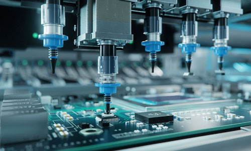
The occurrence of voiding is often related to the soldering process and environmental control. During reflow soldering, if the flux does not volatilize completely or the soldering temperature is insufficient, gases within the solder cannot escape in time, forming voids inside the solder joints. These voids can reduce the mechanical strength and electrical conductivity of the solder joints, potentially leading to poor connections or open circuits in severe cases. Furthermore, environmental humidity is also a potential source of voids. If a PCBA is exposed to a humid environment for too long, the substrate or component surfaces will adsorb moisture. During high-temperature soldering, this moisture rapidly vaporizes into steam; if it cannot escape in time, it forms voids within the solder joints or the substrate. For example, PCBA that has not undergone strict baking to remove moisture is more prone to such issues during soldering.
To address cracking and voiding issues, comprehensive prevention and control measures are needed from three aspects: design, process, and environment. During the design phase, priority should be given to selecting high-Tg substrate materials, and components should be arranged reasonably according to the usage scenario to avoid stress concentration; simultaneously, sufficient mechanical buffer space should be预留 to enhance impact resistance. Regarding process control, the soldering temperature profile must be strictly set to ensure full flux volatilization and uniform solder flow; for humid environments, the PCBA must be thoroughly baked to remove moisture before soldering, reducing interference from water. Environmental management is equally critical; the production workshop must maintain constant temperature and humidity to minimize the impact of dust and static electricity. During transportation and storage, anti-vibration packaging should be used to prevent mechanical damage.
Although the causes of cracking and voiding in PCBA are complex, through scientific material selection, precise process control, and strict environmental management, the risks can be effectively reduced, enhancing product stability and reliability.


No. 501, Industrial North Area, Xinhé Community, Fuhai Subdistrict, Bao'an District, Shenzhen City, Guangdong Province, China